
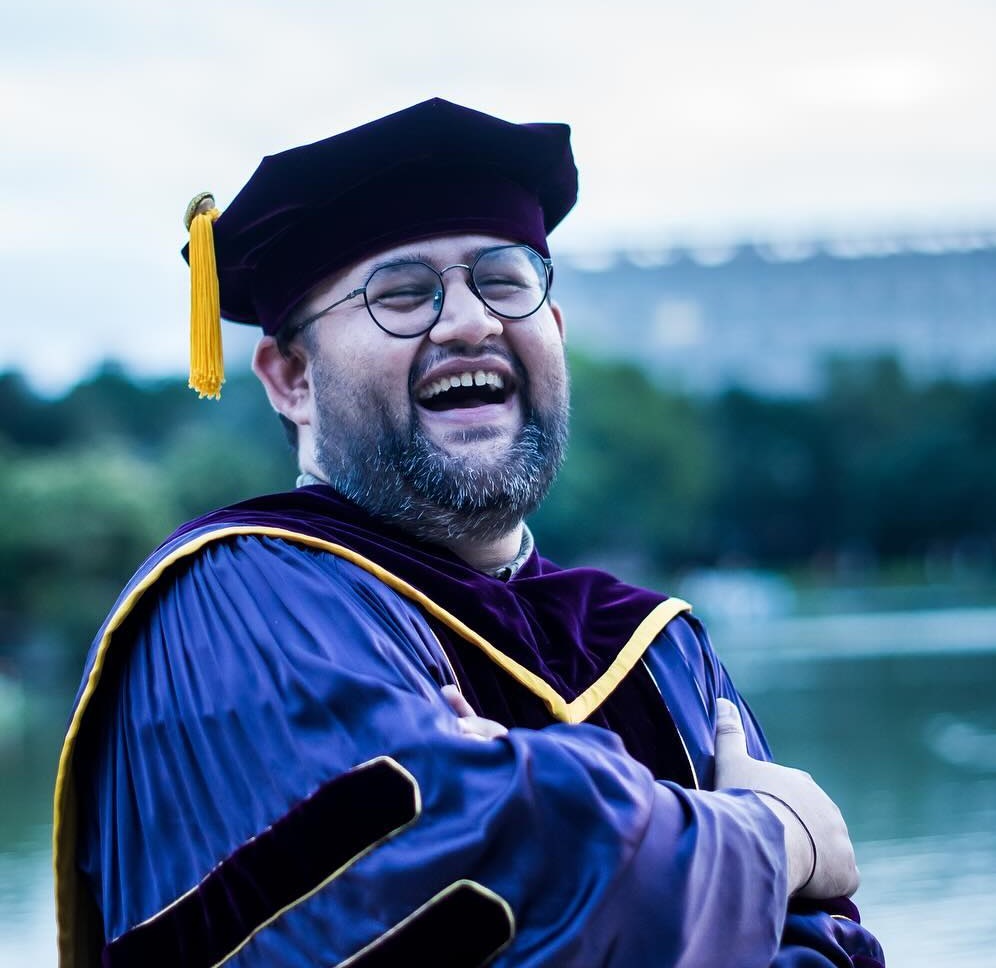
Sandipan Mallik,
PhD
I'm Professor
Professor, Department of Electronics Communication Engineering, NIST University, Pallur Hills, Berhampur, Orissa, India, PIN: 761008.
About
Engineering at NIST University, with a strong focus on semiconductor device physics and advanced material sciences. With over a decade of experience in teaching, research, and mentoring, I have guided numerous students toward prestigious graduate programs and research careers. My expertise spans semiconductor fabrication, lab setup, and collaborative projects aimed at advancing India's semiconductor ecosystem. With over 90 publications and 7 patents, I am dedicated to fostering innovation and supporting the next generation of engineers in cutting-edge technology fields
Research Area:
Specialization: Semiconductor Device Physics, Thin film physics, Device Fabrication Technology, Nanotechnology & Microelectronics, High-k dielectric
Current Area of Research: Thin Film Physics and Technologies, Memristor devices, PAAO template for nanofabrication, PDMS base fabrication, Inorganic heterojunction solar cells, Proteotronics Devices, Biomedical Devices

Empowering India's Semiconductor Future Through Academic Excellence.
The implementation of semiconductor related courses in academic institutions serves as a strategic move towards realizing India's dream of becoming a global electronics hub. The incorporation of these courses enhances students' resumes, equips them with specialized skills for the electronics industry, and aligns them with the nation's vision of technological advancement. By fostering industry-academia collaborations and inspiring high-level research, these courses catalyze India's journey towards self-reliance in semiconductor technologies and position it as a dominant player in the global semiconductor landscape.
Indian Patents
2 Granted
5 Published
Journals
SCI/SCIE: 33
(Q1: 11, Q2: 14, Q3: 08)
Edited Book SCOPUS indexed
Book Chapters SCOPUS indexed
Conference
International: 40
National: 10
Google Scholar Citation
Since 2019: 178
h-index
Since 2020: 8
i10-index
Since 2020: 6
Skills
Software Skill Set:
-
Silvaco, CST Microwave, SCAPS, AMPS-1D, PC-1D, AFORS-HET, Origin Lab, Comsol multiphysics, Matlab, C++, HTML Website Design
1 year Diploma in Computer Programming and Application from All India Society for Electronics and Computer Technology (AISECT) [July 2000 to June 2001]
Equipment Skill Set:
-
High Temperature Furnaces: Tempress Oxidation and diffusion furnaces, Thermolyne 21100 Tube Furnace
Rapid Thermal Annealing: ULVAC-RIKO MILA-3000, MILA-5000
Thin film deposition: RF Sputter: Techtronics, HHV BC 500. DC Sputter: CRESSINGTON SPUTTER COATER 108auto. E-beam Evaporation: Varian. Metallization: HHV
Film Characterization: AFM & SPM: Nanosurf Easyscan2, STM: Nanosurf Easyscan2/ Namma STM i2N Technology
Semiconductor Test System: Agilent E4980A, Agilent 4156C, Agilent B1500A, Keithley 2604B. Semi-automated probe station
Optical: AAA Solar simulator: Newport UV-Vis: Shimadzu UV-1800 FTIR: Agilent Cary 630
Resume
Teaching Area
Subject(s)
PhD:
M.Tech:
M.Sc Physics:
B.Tech:
B.Sc Physics:
Education
Ph.D (Doctor of Philosophy)
Department of Electronics & Telecommunication Engineering, Jadavpur University, Kolkata, India
Thesis Title: “Deposition and Characterization of Hafnium based High-k Gate Dielectrics on SiGe Heterolayers”
M. Tech. (Master of Technology)
Electronics Communication Engineering, Department of ECE, Gandhi Institute of Engineering and Technology (GIET) University, Gunupur, Odisha, India
Project: “Design, Fabrication and Characterization of Iron Disilicide Heterojunction Solar Cells”
M. Sc. (Master of Science)
Physic (Electronics Special Paper), Department of Physics, D.P.Vipra PG College, Bilaspur. (Affiliated to G. G. University, Bilaspur), Chhattisgarh, India
Project: “Fermi Energy Determination of Copper and Silver by Studding Resistance Variation at Different Temperature"
B. Sc. (Bachelor of Science)
Physic (Hons.), Department of Physics, Jhargram Raj College (Affiliated to Vidyasagar University), Jhargram, West Bengal, India
Project: “Effect of Electric Field on the Growth of Sprout-Length of Pea Seeds”
Experience (Academic)
Professor (May 2025 - Present)
Department of Electronics Communication Engg., NIST Berhampur, Orissa, 761008
Associate Professor (April 2019 - April 2025)
Department of Electronics Communication Engg., NIST Berhampur, Orissa, 761008
Assistant Professor (July 2014 - March 2019)
Department of Electronics Communication Engg., NIST Berhampur, Orissa, 761008
Project Scholar (August 2008 - June 2014)
Department of E & ECE, IIT Kharagpur, WB, India, 721302
Contractual Lecturer (June 2007 - July 2008)
Department of Physics, Jhargram Raj College (Govt. of WB), Jhargram, WB, 721507
Experience (Adminstrative/Other)
Coordination of Higher Education Admissions
2025 - Till date
Responsibility: lead and coordinate all university-wide efforts to support NIST students in higher-education admissions and internship opportunities, both in India and abroad
Member: NIST University Academic Committee
2024 - Till date
Responsibility: For overseeing the course curriculum for all programs (UG,PG and Ph.D) across the University
Research and Innovation Coordinator
2021 - 2024
Responsibility: Responsibility: Involved overseeing the institute’s entire research ecosystem by formulating robust R&D policies and fostering a culture of innovation, encouraged faculty members to engage in impactful research and established patent policies to protect and promote intellectual property, devised strategies to guide students toward research excellence, supporting their pursuit of higher studies at premier Indian and international universities, implemented initiatives to boost student research output, organized participation in Hackathons, and nurtured a collaborative environment that stimulated creativity and problem-solving
Member of Board of Studies (BOS)
2018 - Till date
Responsibility: maintaining the academic excellence and growth of the department
NBA Criteria-5/Criteria-1 in charge
2017 - Till Date
Responsibility: secure and maintain NBA accreditation for criterion 5/criterion 1 of Department of ECE
B.Tech Project Coordinator
2016 - 2021
Responsibility: establishing comprehensive project policies that guided the final-year B.Tech students in executing their projects with clear objectives and academic rigor, monitored the progress of those projects, ensuring that students adhered to timelines and maintained high standards in research and development, identified potential projects with strong innovation and market viability, nurturing them through targeted mentorship, actively encouraged students to explore opportunities for transforming their projects into viable startups, fostering a spirit of entrepreneurship and innovation within the institute
NAAC Criteria-3 in charge
2018 - Till Date
Responsibility: secure and maintain NAAC accreditation for criterion 3: Research, Innovations and Extension
NIST Student Counselling Service: Faculty Mentor
2018 - Till date
Responsibility: serves as a crucial support system, helping students succeed academically, personally, and professionally by fostering their overall well-being and development
Google Developer Group on Campus - NIST University:Faculty Mentor
2022 - Till date
Responsibility: support student members in exploring emerging technologies, organizing hands-on workshops, and fostering a collaborative environment for skill development in areas like software engineering, app development, and AI. I work closely with student leaders to shape events and activities that promote technical growth, encourage innovation, and prepare students for real-world challenges in the tech industry
IEEE Student Branch Counselor
2023 - Till date
Responsibility: guide, mentor, and oversee the activities of the IEEE Student Branch, fostering professional growth, technical engagement, and leadership development among its student members.
SPOC Smart India Hackathon
2022 - Till date
Responsibility: facilitated communication between the organizing committee and our institution, ensuring smooth participation for our students in this nationwide innovation event
Activities
Professional Activities
1. KeyNote Speaker of the Joint International Conference on Research and Innovation Smart and Sustainable Solutions in Electrical, Communication and Biomedical Engineering, organized by KSR College of Engineering and The INTI International University, Malaysia, on 26th - 27th March 2026 https://s3conference.ksrce.ac.in/
2. Tutorial Chair of the 1st IEEE International Conference on Air Defense and Security (ICADS-26), organized by NIST University and The Army Air Defence College, Gopalpur, on 12th-13th February 2026 https://www.nist.edu/conference/icads-26/index.html
3. Jury member of the "Hack the Future: AI, DeepTech & IoT Innovation Challenge 2025" , organized by Startup Odisha at O-Hub, Bhubaneswar, on 1st and 2nd December 2025.
4. Jury member of the “ Startup & Innovation Competition”, organized by Khallikote Unitary University, Berhampur, Ganjam, Odisha, on 25th August 2025.
5. Jury member for the “Technical Poster Competition” at Parla Maharaja Engineering College (PMEC), Berhampur, Odisha, organised as a part of the BPUT Tech Carnival 2024, on 18th November 2024
6. Co-convener of International Conference on Technology Advances for Green Solutions and Sustainable Development (ICT4GS-2024) organized by NIST Berhampur (Autonomous) Odisha on 9th and 10th August 2024 at NIST Berhampur (Autonomous) Odisha https://www.ict4gs.in/
7. Co-convener of DST SERB sponsored International Conference on Artificial Intelligence of Things for Sustainability (AIoT4S-2024), organized by NIST Berhampur (Autonomous) Odisha on 20th and 21st January 2024 https://www.nist.edu/conference/aiot4s2024/
8. Co-convener of National Conference Energy, Sustainability and Society (NCESS 2022), organized by NIST Berhampur (Autonomous) Odisha and Indian Energy Congress (IEC) on 10th December 2022 at NIST Berhampur (Autonomous) Odisha. http://nist.edu/conference/ncess2022/
9. Organizing Committee Member; 10th IEEE EDS Mini Colloquium, National Institute of Science and Technology, Palur Hills, Berhampur, Orissa, 20th February 2020.
10. Organizing Committee Member; 8th IEEE EDS Mini Colloquium, National Institute of Science and Technology, Palur Hills, Berhampur, Orissa, 23rd February 2018.
11. Organizing Committee Member; 7th IEEE EDS Mini Colloquium, National Institute of Science and Technology, Palur Hills, Berhampur, Orissa, 6th March 2017.
12. Organizing Committee Member; 3rd National Conference on Devices and Circuits, National Institute of Science and Technology, Palur Hills, Berhampur, Orissa, 7th March 2017.
13. Session Chair; 4th International Conference on Signal and Data Processing 2024, VIT Bhopal, Madhya Pradesh, India, 21-22 November 2024.
14. Session Chair; 3rd International Conference on Signal and Data Processing 2023, VIT Bhopal, Madhya Pradesh, India, 3-4 November 2023.
15. Session Chair; of Topical/Vertical Sessions entitled
“Energy efficiency and energy harvesting in IoT” of the IEEE Future Networks World Forum, Montreal, Canada, October 2022.
16. Session Chair; International Conference on Computational Techniques and Applications 2021, WINAR Charitable trust, IETE, Kolkata & The electro inventor, Kolkata, India, 9-10 Octomber 2021.
17. Session Chair; 4th National Conference on Devices and Circuits, National Institute of Science and Technology, Palur Hills, Berhampur, Orissa, 24th February 2018.
18. Session Chair; 2nd National Conference on Devices and Circuits, National Institute of Science and Technology, Palur Hills, Berhampur, Orissa, 19th February 2016.
19. Summer training (200 hours) course coordinator cum instructor of "Nano Electronics: Design and Fabrication (NEDF)", National Institute of Science and Technology, Palur Hills, Berhampur, Orissa, 2015, 2017, 2018.
Guest Lecture/Talk
1. KeyNote Speaker of the Joint International Conference on Research and Innovation Smart and Sustainable Solutions in Electrical, Communication and Biomedical Engineering, organized by KSR College of Engineering and The INTI International University, Malaysia, on 26th - 27th March 2026 https://s3conference.ksrce.ac.in/
2. Guest Talk on “Smart Simplicity: The Art of Frugal Innovation” in the 3rd Internship Program organised by Next-Gen Research and Innovation Hub (NGRiH) on 24th October 2025.
3. Chief Speaker for the “Awareness Program on Startup & Innovation Competition”, organized by Khallikote Unitary University, Berhampur, Ganjam, Odisha, on 22nd August 2025.
4. Guest talk on “From Research Question to Review Paper: A Practical Guide to Research Methodology” organized by the IQAC Cell of Government Science College, Chatrapur, Ganjam, Odisha, on 3rd May 2025.
5. Keynote Speaker at the “International Conference on Emerging Issues in Computer Applications (EICA - 2025)” organized by K. S. R College of Engineering, Tiruchengode, Tamil Nadu, on 28th March 2025.
6. Guest talk on “Advanced Research Writing Techniques for Emerging Trends in Electrical Systems” during the 5-day Online Faculty Development Program organized by Department of Electrical & Electronics Engineering, Stanley College of Engineering & Technology for Women, Hyderabad, Telangana., on 25th October 2024.
7. Guest talk on "Reference Management using Mendeley" during the online workshop "Research Writing with LaTeX and Mendeley," organized by the Consortium for Next Generation Research and Innovation (C4NGRI) on 17th July 2024.
8. Guest talk on “Intellectual Property Rights (IPR)” on World Intellectual Property Day organised by Sankalp Senior Secondary School, Berhampur, Odisha on 29th April, 2024.
9. Guest talk on "Reference Management using Mendeley" during the Faculty Development Program (FDP) on Systematic Literature Review and Bibliometric Analysis (SLR and BA-2024) organized by Dept. of Management Studies, NIST University on 26th January 2024 on 4th January 2024.
10. Guest talk on “Intellectual property rights: Importance & Scope” at Virtual short term Course entitled “Research Trends in Electronics and Communication Engineering-2021” organized by University College of Engineering and Technology, Vinoba Bhabe University, Hazaribag, Jharkhand under TEQUIP III, on 9th February 2021.
11. Guest talk on “Modelling and Simulation of Heterojunction Solar Cells” at Virtual short term Course entitled “Research Trends in Electronics and Communication Engineering-2021” organized by University College of Engineering and Technology, Vinoba Bhabe University, Hazaribag, Jharkhand under TEQUIP III, on 8th February 2021.
12. Guest talk on “Templated Synthesis of Nanorod Arrays" at International Seminar on Recent Advances in Physics [RAP], organized by Dept. of Physics, Jhargram Raj College & Jhargram Raj College Physics Alumni Association on 21st December 2019.
13. Guest talk on “e-Breadboard: A General Purpose DC Emulator”, A one day International Seminar on Impact of Physical Science in Society (IPSS), organized by Dept. of Physics, Jhargram Raj College, Govt. of W.B. & Jhargram Raj College Physics Alumni Association, July 20, 2018.
14. Guest talk on “Patents: What You Should Knows", 2nd-Physics Alumni Meet, Department of Physics, Jhargram Raj College (Under Vidyasagar University) Jhargram, West Bengal, December 22, 2017.
15. Guest talk on "Metal Oxide Semiconductor with High-K Gate Dielectrics", Electronics & Communication Engineering Gandhi Institute for Education & Technology Baniatangi, Bhubaneswar, Khurda – 752060, September 10, 2016.
Faculty Development Program (6 days or more)
1. Participated in One Week ISTE approved Online Faculty Development Program on “Intellectual Property Rights” organized by Cummins College of Engg For Women, Hingna, Nagpur, March 07-12, 2022.
2. Participated in Two weeks Training Program for Faculty Members on AICTE Students Learning Assessment (PARAKH) in collaboration with CIDC, under the auspices of AICTE, GOI, January 10-23, 2022.
3. Participated in One week National e-workshop on Innovation & Intellectual Property Rights, conducted by CSIR-IMMT Bhubaneswar, June 14-19, 2021.
4. Completed Eight weeks NPTEL Online Certification course entitled "Roadmap of Patent Creation" with score of 87%, from Jan-Mar 2021.
5. Participated in One week Faculty Development Programme on “VLSI Chip Design Hands-on using Open Source EDA” jointly organized by Electronics and ICT Academies through National Knowledge Network under the “Scheme of financial assistance for setting up pf Electronics and ICT Academies” of the Ministry of Electronics and Information Technology (MeitY), Gove of India from 08th to 12th July, 2019.
6. Participated in One week Faculty Development Programme on “Robotics & AI” jointly organized by Electronics and ICT Academies through National Knowledge Network under the “Scheme of financial assistance for setting up pf Electronics and ICT Academies” of the Ministry of Electronics and Information Technology (MeitY), Gove of India from 24th to 28th June, 2019.
7. Participated in One week Faculty Development Programme on “DSP & Sensors” jointly organized by Electronics and ICT Academics through National Knowledge Network under the “Scheme of financial assistance for setting up pf Electronics and ICT Academies” of the Ministry of Electronics and Information Technology (MeitY), Gove of India from 10th to 14th December, 2018.
8. Participated in Two weeks ISST STTP at National Institute of Science and Technology, Palur Hills, Berhampur, Orissa, 761008 on "CMOS, Mixed Signal and Radio Frequency VLSI Design", Conducted by Indian Institute of Technology Kharagpur, from 26th December to 4th February, 2017.
Conference, Seminar, Workshop (Attended)
1. Participated in 6th National Level Online Workshop on “NIRF India Rankings 2025” for Higher Educational Institutions held on 20th & 21st December, 2024 through, conducted by Institute for Academic Excellence (IAE), Hyderabad.
2. Particioated in 2 days Faculty Developement Programme on “Learning Strategies for Vibrant Teaching” conducted by Indian Institute of Public Administration on February 6-7, 2024.
3. Completed 4 hrs. Distance learning course on “Introduction to the Patent Cooperation Treaty (PCT101E20)" on 26 July 2020, organized by WIPO ACADEMY.
4. Completed 8 hrs. distance learning course on "e-Tutorial on using Patent Information (DL177E20S1)" on 25 July 2020, organized by WIPO ACADEMY.
5. Webinar session on Concepts, Innovations and Methods when Chemistry meets Biology, organized by Department of Chemistry, Kharagpur College, Kharagpur, W.B., on 17-07-2020.
6. Webinar session on Emerging Trends in Genetic Engineering, organized by Department of Biochemistry/Biotech/Microbiology, Chaitanya Deemed to be University on 30-06-2020.
7. Webinar session on "Quantum World: Past, Present & Future", organized by Dept of Physics, P. K. College, Contai, W.B., on 03-07-2020, 08-07-2020 and 11-07-2020
8. Webinar session on Evolution of Texture in Materials delivered by Dr. Ajit Panigrahi, organized by Department of Mechanical Engineering, NIST Berhampur on 18-06-2020.
9. Webinar session on Connecting Engineering to MEP Industry, organized by Dhanush Engg Services Ltd., approved by NSDC, on , on 18-06-2020.
10. Webinar session on Materials Characterization using Time of Flight Secondary Ion Mass Spectroscopy (TOF-SIMS) delivered by Dr. Manas Kumar Dalai, organized by Department of Mechanical Engineering, NIST Berhampur on 17-06-2020.
11. Participated in 2 days “National Workshop on LATEX” organizes by School of Computer Science & Engineering, National Institute of Science and Technology, Palur Hills, Berhampur, Orissa, held on 24th to 25th November 2017.
12. Participated in 2 days workshop on “Innovative Research in Pedagogy for Mini-MOOCs Blended with Instruction Strategies to Enhance Quality of Higher Education” under Newton Bhaba research project by Royal Academy of Engineering, UK at National Institute of Science and Technology, Palur Hills, Berhampur, Orissa, held on 19th & 20th August 2017.
13. Participated in 6th IEEE EDS Mini Colloquium, National Institute of Science and Technology, Palur Hills, Berhampur, Orissa, 20th February 2016.
14. Participated in 5th IEEE EDS Mini Colloquium, National Institute of Science and Technology, Palur Hills, Berhampur, Orissa, 19th December 2015.
15. Participated in “Engineering Faculty Workshop” conducted by National Institute of Science and Technology, Palur Hills, Berhampur, Orissa, 761008 of WIPRO Mission 10X program, 2nd-4th December 2014.
16. Participated 21st International Symposium on the Physical & Failure Analysis of Integrated Circuits (IPFA 2014), Marina Bay Sands Hotel, Singapore, 30 June to 4 July 2014.
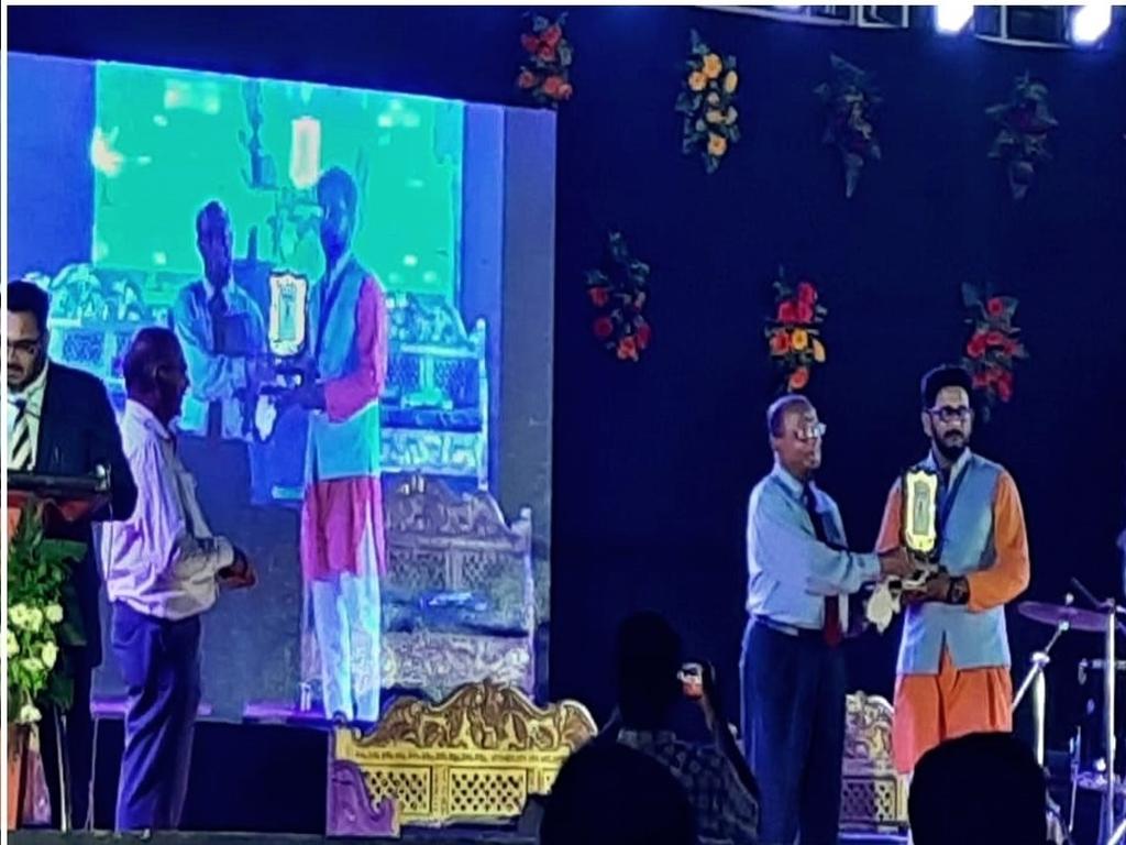
Awards
NIST Foundation Day Research Award
During the 28th NIST foundation day Research Award for outstanding research contribution in corresponding domain, January 2025
NIST Foundation Day Academic Excellence Award
During the 28th NIST foundation day Academic Excellence Award for exceptional dedication to teaching and mentoring students, January 2025
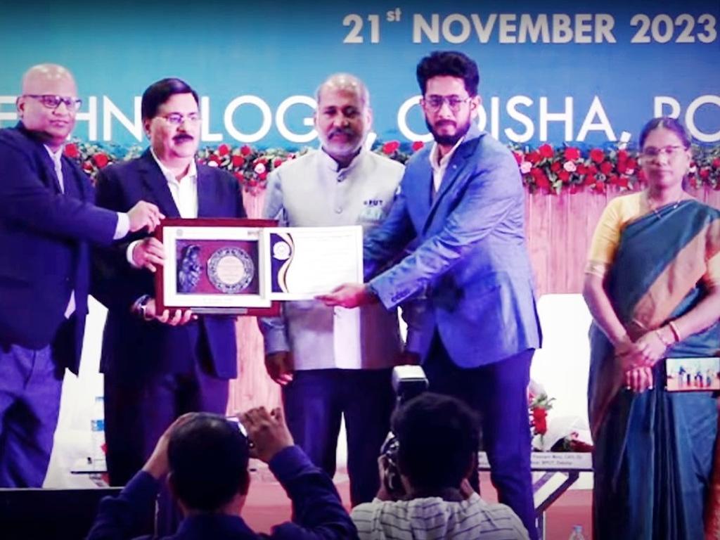
BPUT Foundation Day Research Award
In ECE, during the 22nd foundation day of Biju Patnaik University of Technology (BPUT) for outstanding research contribution in corresponding domain, November 2023
NIST Faculty Excellence Award
Faculty Excellence Award for outstanding contribution in teaching and research by NIST Berhampur, October 2021.
Mentor of CSIR-SRTP
Non-CSIR Mentor of CSIR-SUMMER RESEARCH TRAINING PROGRAMME-June-August 2020
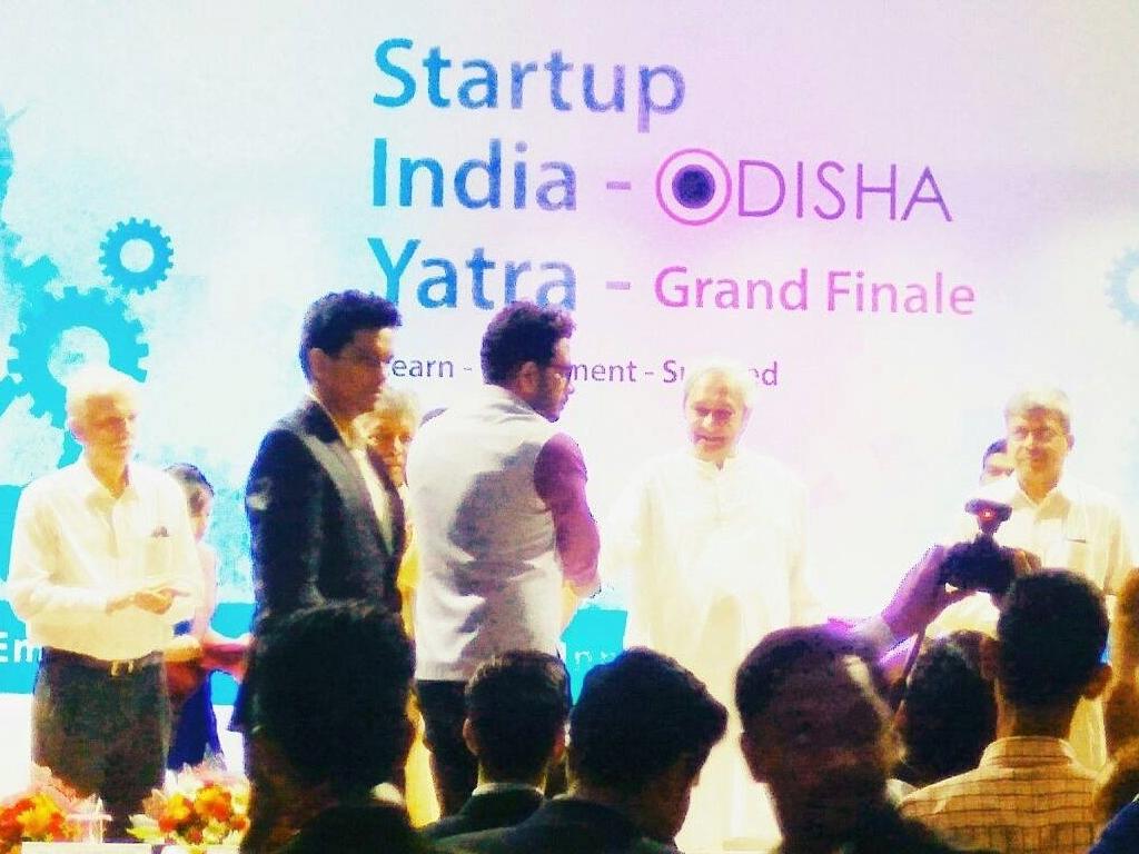
Chief Minister of Odisha Award
For Startup India Odisha Yatra of the project entitled “Low Cost Flexible Capacitive Pressure Sensor”, April 2018
Academic Mentorship
Mentorship in Higher Studies/Research
The following students were directly mentored to pursue their higher education in Indian and foreign universities during their undergraduate studies at NIST Berhampur. Majority of the students achieved their MS/PhD position in the mentioned universities with partial/full scholarship


Mentorship in International Internship
The following students were directly mentored to pursue Summer Research Internship Program (two to three month duration) in Foreign universities during their undergraduate studies at NIST Berhampur. All the selected students achieved their internship position in the mentioned universities with full scholarship


Doctoral Thesis Supervision
The following research scholars are currently pursuing or have successfully completed their doctoral thesis work.
Supervisor
(status: Ongoing)
Partha Pratim Maiti
BPUT Rourkela
Supervisor
(status: Ongoing)
Laxmi Vandana
BPUT Rourkela
Supervisor
(status: Ongoing)
Raja Rajeswari
NIST University
Supervisor
(status: Ongoing)
Sasmita Padhy
NIST University
Co-Supervisor
(status: Ongoing)
Sk. Manowar Ali
GIET University
Publication
Patent:
1. Atanu Jana, M. Tarun, Badal Ritesh Kumar, Kunjabihari Swain, Tapaswini Maharana, S Mallik, “A PORTABLE ANALYTICAL DEVICE FOR IN-SITU DETECTION AND QUANTIFICATION OF MICROPLASTIC PARTICLES IN WATER SAMPLES”, Application no: 202531123805, The Patent Office Journal No. xx/2025 Dated 09/12/2025
2. L Vandana, A Dash, U Dey, S Mahata, S Guhathakurata, S Mallik, G Ahmad, C S Kumar, C Jachob “METHOD FOR PRODUCTION OF TEXTURED FLEXIBLE SOLAR CELLS AND SOLAR CELLS ATTAINED THEREOF”, Application no: 202331013288, The Patent Office Journal No. 13/2023 Dated 31/03/2023
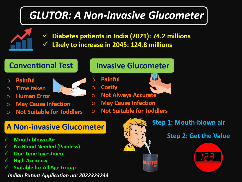
3. S Mallik, D. Panda, P. Panigrahi, A. Dash, “NON-INVASIVE GLUCOMETER TO DETERMINE BLOOD GLUCOSE LEVEL FROM MOUTH-BLOWN AIR AND A METHODE THEREOF” Application no: 202131003286, The Patent Office Journal No. 38/2022 Dated 23/09/2022
4. P. K. Patra, M. Sahu, A. Dash, and S Mallik, “A SINGLE MICROSTRIP ANTENNA AS RADIATOR NAD REFLECTOR”, Application no: 202131002987, The Patent Office Journal No. 08/2021 Dated 19/02/2021 Granted
5. P. Das, A. Singh, S. S. Mahato, S Mallik and M. K. Mandal, "A SYSTEM FOR CUSTOMIZED UNIVERSAL DC CIRCUIT EMULATION AND A METHOD THEREOF"; Application No. 201831035787, The Patent Office Journal No. 13/2020 Dated 27/03/2020 Granted
6. S Mallik, R. Roy, G. Ahmad, A. Raja, S. H. Raheman, A. Dash, P. Panigrahi, P. K. Singh, S. Guhathkurata, N. B. Manik, P. Das and S. S Mahato, "AN AUTOMATED PROBING SYSTEM FOR MEASURING ELECTRICAL CHARACTERISTICS OF ON-WAFER DEVICES ANDA METHOD THEREOF"; Application No. 202031041107, The Patent Office Journal No. 42/2020 Dated 16/10/2020
7. S Mallik, A. Dash, A. Choudhury, P. Das, S. S. Mahato, C. Mahata, A. Bag and C. K. Maiti, "METAL PROTEIN SEMICONDUCTOR STRUCTURE"; Application No. 201831045064, The Patent Office Journal No. 47/2019 Dated 22/11/2019
Journal:
1. P P Maiti, C. Mukherjee, A. Bag, S Mallik, C. K. Maiti, "Defect Characterization of HfTiOx Gate Dielectrics on SiGe Heterolayers Using Inelastic Tunneling Spectroscopy", Journal of Electronic Materials, November 2024 [Q2 SCI, impact factor: 1.9, doi: 10.1007/s11664-024-11550-7] - Accepted
2. S R Panda, M Pradhan, S Mallik, T Sahu, "Asymmetric Doping-Dependent Electron Transport Mobility in InxGa1–xAs/GaAs Quantum Well Field-Effect Transistor Structure", Physica Status Solidi (B), 2400206 pp. 1-8, July 2024 [Q3 SCI, impact factor: 1.6, doi: 10.1002/pssb.202400206]
3. N. Topno, V. Hemaja, D.K.Panda, D K Dash, R Swain, S Mallik & J K Dash, "Performance characterization of Ferroelectric GaN HEMT based biosensor" Microsystem Technologies, May 2024 [Q3, SCI, impact factor: 1.6, doi: 10.1007/s00542-024-05727-7]
4. Laxmi Vandana, Gufran Ahmad, S Mallik, "Enhancement of photon absorption in thin film CdTe solar cell with microtextured quartz substrate, Materials Today: Proceedings, in press, July 2024 [SCOPUS, doi: https://doi.org/10.1016/j.matpr.2024.06.016]
5. L. Vandana, S. Guhathakurata, G. Ahamed and S Mallik, " Design prospect of CdTe solar cell using NW-CdS window layer and 3D graphene as back electrode from numerical approach ", Indian J Phys, May 2024 [Q3 SCI, impact factor: 1.97, doi: 10.1007/s12648-024-03293-2]
6. S Guhathakurata, D Pal, B S Reddy, N B Manik, S Mallik, “Fabrication of Highly Transparent Substrates from Waste Materials for Electronic Device Applications” ACS Applied Electronic Materials, vol. 6, pp. 4080-4089, May 2024 [Q1, SCI, impact Factor: 4.3, doi: https://doi.org/10.1021/acsaelm.4c00144]
7. Y R Yang, T C Liu, Y W Chen, P P Pancham, G Ahmad, S Mallik, and C Y Lo, "Thermoresistive Profile Sensing with Taiji Pattern for Isotropic Strain Detection”, IEEE Sensors Journal,vol. 24, pp. 9506-9513 2024 [Q1, SCIE, impact factor: 4.3 doi: 10.1109/JSEN.2024.3360238]
8. J Y Wu, T Y Hsu, G Ahmad, S Mallik, and C-Y Lo, „Novel Multiaxial Force Decoupling Strategy in Vertically Stacked Force Sensors with Hybrid Fabrication Techniques” IEEE Sensors Journal, vol. 23, pp. 30135-30142, October 2023 [Q1, SCIE, impact factor: 4.3 doi: 10.1109/JSEN.2023.3326310]
9. S Jamkar, A Tripathy, S Mallik, Dipankar Pal, "Methodologies of removal of heavy metals from contaminated water using various waste materials: A comprehensive review, ChemBioEngg Review, vol.10 pp. 1-35 September 2023 [Q1, SCIE, impact factor: 4.8, doi: 10.1002/cben.202300020]
10. P P Pancham, A Mukherjee, B L Yuan, P Yu, W-H Chiu, G Ahmad, S Mallik, C-Y Lo, "Novel graphene transfer method to silicone and its sensing application on porous PDMS", IEEE Sensors Letters, vol. 7, pp. , April 2023 [SCOPUS, doi: 10.1109/LSENS.2023.3265702]
11. 10. S. Mohanty, D. Panda, A. Dash, S. S. Kumar, R. R. Padhi, S. Guhathakurata and S Mallik, "A Review on Borophene: A Potential Gas Capture Material", J. Electron. Mater. vol. 52, pp. 4434–4454, April 2023 [Q2, SCIE, impact factor: 1.9, doi: 10.1007/s11664-023-10367-0]
12. B. S. Reddy, and S Mallik, "Uneven Contact Wear Tribology Test on ZTA Disc with Diamond Tip and ZrO2 Ball", Adv. Mech, July 2023 [SCOPUS, doi:advancesinmechanics.com/1621.php Print ISSN: 1000-0992]
13. Prajukta Mukherjee, Aritra Acharyya & S Mallik, "Bovine Serum Albumin-Based Thin-Film Capacitors for Flexible Electronic Applications" IETE Journal of Research, July 2022 [Q3, SCIE, impact factor: 1.7, doi: 10.1080/03772063.2022.2098183]
14. D. Deo, S. P. Singh, S. Mohanty, S. Guhathakurata, D. Pal and S Mallik, "Biomimicking of Phyto-based Superhydrophobic Surfaces towards Prospective Applications: A Review", Mat. Res. Letter. vol. 57, pp. 8569–8596 April 2022 [Q1, SCIE, impact factor: 4.2, doi: 10.1007/s10853-022-07172-1 ISBN: 1573-4803]
15. S. Mohanty, A. Arya, D. Jena, S. Guhathakurata, N. B. Manik, G. Ahmad and S Mallik, "Potential Soluble Substrates for Transient Electronics Applications: A Review", AIP Avdavces, vol. 12, May 2022, [Q2, SCIE, impact factor: 1.53, doi:10.1063/5.0066174 ISSN: 2158-3226]
16. P. Maiti, Ajit Dash, S. Guhathakurata, S Das, A. Bag, T P Dash, G. Ahmed, C. K. Maiti and S Mallik, “Experimental and Simulation Study of Charge Transport Mechanism in HfTiOx High-k Gate Dielectric on SiGe Heterolayers”, Bull. Mat. Res vol. 45, issue. 1, pp. 1-8, March 2022, [Q3, SCIE, impact factor: 1.7, doi: 10.1007/s12034-021-02622-z ISSN: 0973-7669]
17. A. Dash, A. Sharma, S. K. Jain, B. S. K. Patra, A. Gundimeda, S Mallik and G. Gupta "Influence of current conduction paths and native defects on gas sensing properties of polar and non-polar GaN" Journal of Alloys and Compounds, vol. 898, p. 162808, March 2022 [Q1, SCI, impact factor: 5.36, doi:10.1016/j.jallcom.2021.162808 ISSN: 0925-8388]
18. A. R. Tripathy, A. Choudhury, A. Dash, P. Panigrahi, S. S. Kumar, P. P. Pancham, S. K. Sahu, and S Mallik, Polymer Matrix Composite Engineering for PDMS based Capacitive Sensors to achieve high-performance and broad-range Pressure Sensing, Appl. Surf. Sci. Adv., vol. 3, pp. 100062, March 2021. [SCOPUS doi: https://doi.org/10.1016/j.apsadv.2021.100062 ISSN: 2666-5239]
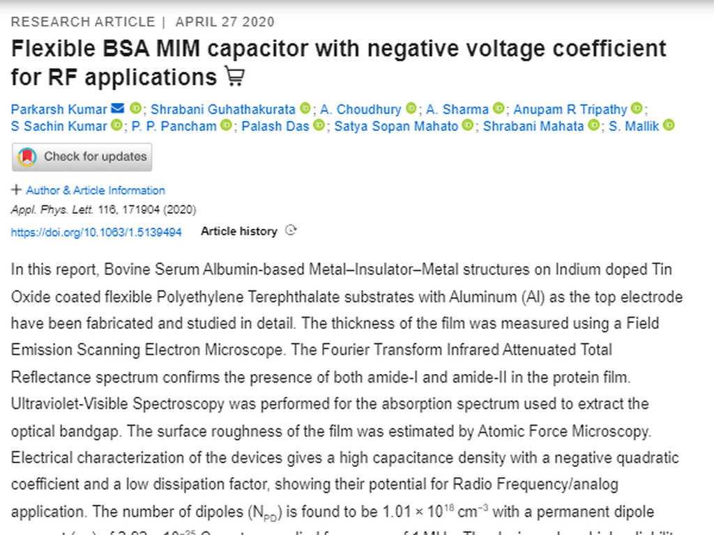
19. P. Kumar, A. Choudhury, S. Guhathakurata, A. Sharma, A. R. Tripathy, S S. Kumar, P. P. Pancham, P. Das, S. S. Mahato, S. Mahata, S Mallik, "Flexible BSA MIM Capacitor with Negative Voltage Coefficient for RF Applications", Appl. Phys. Lett. vol. 116, issue. 17, pp. 1719041-1719045, April 2020 [Q1, SCI, impact Factor: 3.52, doi: https://doi.org/10.1063/ 1.5139494 Print ISSN: 0003-6951, Online ISSN: 1077-3118]
20. P. Das, S. K Jana, N. N. Halder, S Mallik, S. S. Mahato, A. K. Panda, P. P. Chow, D. Biswas, "An alternative X-Ray Diffraction analysis for comprehensive determination of structural properties in compositionally graded strained AlGaN epilayers" Electron Mater Lett, vol. 14, pp. 784-792, November 2018. [Q2, SCIE, impact factor: 2.882, doi: 10.1007/s13391-018-0074-6 Online ISSN 2093-6788, Print ISSN 1738-8090]
21. S. P. Mallick, D. P. Dash, S Mallik, R. Roshan, S. Mahata, P. Das and S. S. Mahato, “An Empirical Approach towards Photovoltaic Parameter Extraction and Optimization”, Solar Energy, vol. 153, pp. 360-365, June 2017. [Q1, SCI, impact factor: 4.37, doi: 10.1016/j.solener.2017.05.076 ISSN: 0038-092X]
22. D. P. Dash, R. Roshan, S. Mahata, S Mallik, S. S. Mahato and S. K. Sarkar, “A compact J-V model for solar cell to simplify parameter calculation”, J. Renewable Sustainable Energy vol. 7, issue 1, pp. 0131271-0131277, February 2015. [Q3, SCIE, impact factor: 1.33, doi: 10.1063/1.4909540 ISSN: 1941-7012]
23. A. Bag, S Mallik and C. K. Maiti, "Interlayer thickness dependence of photovoltaic properties of polycrystalline p-β-FeSi2(Al)/n-Si(100) heterojunctions," J. Renewable Sustainable Energy, vol. 6, no. 2, pp. 023110-023112 , March 2014. [Q3, SCIE, impact factor: 1.33, doi: 10.1063/1.4871285 ISSN: 1941-7012]
24. M. K. Hota, A. Bag, S Mallik, S. Verma, and C. K. Maiti, “Resistive Switching in ITO/Graphene Oxide/Al Metal-Insulator-Metal Capacitor Structures,” Graphene, vol. 1, no. 1, pp. 45-50, June 2013 doi: 10.1166/graph.2013.1010 Print ISSN 2167-275X; Online ISSN 2167-2768]
25. A. Bag, M. K. Hota, S Mallik, and C. K. Maiti, “Graphene oxide-based flexible metal–insulator–metal capacitors,” Semiconductor Science and Technology, vol. 28, no. 5, pp. 055002-055002-7, March 2013. [Q2, SCI, impact factor: 2.28, doi: 10.1088/0268-1242/28/5/055002 Online ISSN: 1361-6641, Print ISSN: 0268-1242]
26. S Mallik, C. Mukherjee, C. Mahata, M. K. Hota, T. Das, G. K. Dalapati, H. Gao, M. K. Kumar, D. Z. Chi, C. K. Sarkar, and C. K. Maiti, “Electrical properties and noise characterization of HfO2 gate dielectrics on strained SiGe layers,” Thin Solid Films, vol. 522, no. 1, pp. 267-273, November 2012. [Q2, SCI, impact factor: 1.93, doi: 10.1016/j.tsf.2012.07.111 ISSN: 0040-6090]
27. C. Mahata, S Mallik, T. Das, C. K. Maiti, G.K. Dalapati, C.C. Tan, C.K. Chia, H. Gao, M. K. Kumar, S. Y. Chiam, H. R. Tan, H. L. Seng, D. Z. Chi, and E. Miranda, “Atomic layer deposited (TiO2)x(Al2O3)1-x/In0.53Ga0.47As gate stacks for III-V based metal-oxide-semiconductor field-effect transistor applications”, Appl. Phys. Lett., vol. 100, no. 6, pp. 062905-062905-4, February 2012. [Q1, SCI, impact factor: 3.49, doi: 10.1063/1.3684803 Print ISSN: 0003-6951, Online ISSN: 1077-3118]
28. T. Das, C. Mahata, S Mallik, S. Varma, G. Sutradhar, P.K. Bose, and C. K. Maiti, “Interface Properties of Mixed (TiO2)1−x(Y2O3)x and (Ta2O5)1−x(Y2O3)x (0≤ x≤ 1) Gate Dielectrics on Sulfur-Passivated GaAs”, Journal of The Electrochemical Society, vol. 159, no. 3, pp. H323-H328, January 2012. [Q1, SCI, impact factor: 3.66, doi: 10.1149/2.094203jes Print ISSN: 0013-4651, Online ISSN: 1945-7111]
29. M. K Hota, S Mallik, C. K. Sarkar, S. Varma, and C. K. Maiti, “Structural and Electrical Properties of Radio Frequency Sputtered HfTaOx Films for High-k Gate Insulator”, Japanese Journal of Applied Physics, vol. 50, no. 10, pp. 101101-101101-5, October 2011. [Q2, SCI, impact factor: 1.45, doi: 10.1143/JJAP.50.101101 Online ISSN: 1347-4065, Print ISSN: 0021-4922]
30. S Mallik, C. Mahata, M. K. Hota, C. K. Sarkar, and C. K. Maiti, "Si1-xGex metal-oxide-semiconductor capacitors with HfTaOx gate dielectrics," Thin Solid Films, vol. 520, no. 1, pp. 101-105, October 2011. [Q2, SCI, impact factor: 1.93, doi: 10.1016/j.tsf.2011.06.057 ISSN: 0040-6090]
31. C. Mahata, T. Das, S Mallik, M. K. Hota, and C. K. Maiti, “Chemical Bonding States of Plasma Nitrided High-k/Ge Gate Stack,” Electrochemical and Solid-State Letters, vol. 14, no. 4, pp. H167-H170, April 2011. [Q2, SCI, impact factor: 2.31, doi: 10.1149/1.3545937 Print ISSN: 1099-0062, Online ISSN: 1944-8775]
32. C Mahata, S Mallik, T Das, MK Hota, C. K. Maiti, “Interface Structure and Charge Trapping in Hf-Incorporated Y2O3 Gate Dielectrics on Germanium”, ECS Transactions, vol. 35, no. 4, pp. 835-845, April 2011 [SCOPUS,doi: 10.1149/1.3572322 Print ISSN: 1938-6737, Online ISSN: 1938-5862]
33. S Mallik, C. Mahata, M. K. Hota, G. K. Dalapati, H. GaO, M. K. Kumar, D. Z.Chi, C. K. Sarkar, and C. K. Maiti, “Electrical Properties of SiGe MOS Capacitors with Ultrathin ALD Hafnium Dioxide,” ECS Transactions, vol. 35, no. 3, pp. 513-520, April 2011 [SCOPUS, doi: 10.1149/1.3569942 Print ISSN: 1938-6737, Online ISSN: 1938-5862]
34. C. Mahata, T. Das, S Mallik, M. K. Hota, S. Varma, and C. K. Maiti, “Flatband Voltage Characteristics of Hf-incorporated Y2O3/strained-Si Gate Stacks with Au, Pt, and Ni Metal Gates,” Electrochemical and Solid-state Letters, vol. 14, no. 2, pp. H80-H83, February 2011. [Q2, SCI, impact factor: 2.31, doi: 10.1149/1.3516638 Print ISSN: 1099-0062, Online ISSN: 1944-8775]
35. M. K. Hota, C. Mahata, S Mallik, C. K. Sarkar, and C. K. Maiti, “Impact of Top (Pt, Au, and Al) Electrodes on HfAlOx-Based MIM Capacitors,” Journal of The Electrochemical Society, vol. 158, no. 1, pp. H44-H49, January 2011. [Q1, SCI, impact factor: 3.66, doi: 10.1149/1.3514656 Print ISSN: 0013-4651, Online ISSN: 1945-7111]
36. M. K. Hota, S Mallik, C. K. Sarkar, and C. K. Maiti, “Temperature dependence of TaAlOx metal-insulator-metal capacitors,” Journal of Vacuum Science and Technology B, vol. 29, no. 1, pp. 01AC06-01AC06-5, January 2011. [Q3, SCI, impact factor: 1.31, doi: 10.1116/1.3535558 ISSN: 1071-1023]
37. S Mallik, C. Mahata, M. K. Hota, G. K. Dalapati, D. Chi, C. K. Sarkar, and C. K. Maiti, “HfAlOx high-k gate dielectric on SiGe: Interfacial reaction, energy-band alignment, and charge trapping properties,” Microelectronic Engineering, vol. 87, no. 11, pp. 2234-2240, November 2010. [Q2, SCI, impact factor: 1.91, doi: 10.1016/j.mee.2010.02.009 ISSN: 0167-9317]
38. M. K. Hota, C. Mahata, M. K. Bera, S Mallik, C. K. Sarkar, S. Verma, and C. K. Maiti, “Preparation and characterization of TaAlOx high-κ dielectric for metal–insulator–metal capacitor applications,” Thin Solid Films, vol. 519, no. 1, pp. 423-429, October 2010. [Q2, SCI, impact factor: 1.93, doi: 10.1016/j.tsf.2010.07.020 ISSN: 0040-6090]
39. C. Mahata, M. K. Bera, M. K. Hota, T. Das, S Mallik, B. Majhi, S. Verma, P. K. Bose, and C. K. Maiti, “High performance TaYOx-based MIM capacitors,” Microelectronic Engineering, vol. 86, no. 11, pp. 2180-2186, November 2009. [Q2, SCI, impact factor: 2.02, doi: 10.1016/j.mee.2009.03.025 ISSN: 0167-9317]
40. C. Mahata, M. K. Bera, T. Das, S Mallik, M. K. Hota, B. Majhi, S. Verma, P. K. Bose, and C. K. Maiti, “Charge trapping and reliability characteristics of sputtered Y2O3 high-k dielectrics on N- and S-passivated germanium,” Semiconductor Science and Technology, vol. 24, no. 8, pp. 085006-1-8, July 2009. [Q2, SCI, impact factor: 2.28, doi: 10.1088/0268-1242/24/8/085006 Print ISSN: 0268-1242, Online ISSN: 1361-6641]
41. C. Mahata, M. K. Bera, S Mallik, B. Majhi, M. K. Hota, T. Das, S. Verma, and C. K. Maiti, “Charge Trapping Characteristics of TaYOx Gate Dielectrics on Ge under DC and AC Stressing,” ECS Transactions, vol. 19, no. 2, pp. 699-710, May 2009 [SCOPUS, doi: 10.1149/1.3122125 Print ISSN: 1938-6737, Online ISSN: 1938-5862]
42. Alok Chattaraj, S Mallik, Tapati Das and A. Ghorai, "Effect of electric field and potential on the Germination of gram and pea seeds," Physics Education, vol. 25, no. 1, pp. 05-10, 2008 http://physics.unipune.ac.in/~phyed/25.1.html ISSN 0970-5953]
Book (Edited):
1. International Conference on Technology Advances for Green Solutions and Sustainable Development, B K Mishra, Alvaro Rocha, S Mallik, Springer Nature, 2024 (DOI: 10.1007/978-3-031-94997-5)
This volume collects peer-reviewed papers from the ICT4GS-2024 conference, offering multidisciplinary insights into how emerging technologies—such as IoT, AI and blockchain—can support sustainable development, renewable energy, smart cities and circular economy strategies. It serves as a resource for researchers, practitioners and policymakers seeking to explore the intersection of green solutions and digital innovation for environmental resilience.
2. Smart Sensors for Industry 4.0: Fundamentals, Fabrication and IIoT Applications, B K Mishra, S Mallik, D N Le, Wiley, 2023 (DOI: 10.1002/9781394214723)
Industry 4.0, powered by IoT, big data, cloud computing, AI, machine learning, and smart sensors, is transforming conventional production systems.The book entitled Smart Sensors for Industry 4.0: Fundamentals, Fabrication, and IIoT Applications bring together the latest research in materials and methodology for the fabrication of intelligent sensors, its IoT system integration, and IIoT applications to promote a vision towards making a smart industry.
Book Chapters:
1. S S Kumar, D Panda, RR Padhi, VRK Patro, SR Dash, K Kashyap, TK Giri, D Mishra, S Mallik "A Low-Cost Advanced Device for the Detection of Pesticides with NDVI Method" Intelligent Technologies for Sensors: Applications, Design, and Optimization for a Smart World, P 181, CRC Press 2023 [ISBN:978-1-77491-185-3] June 2023
2. M Suresh, S Mallik, Y Kumar, O S Rao, M Singh, D Adhikary, S S Patnaik, M R Sahu "IoT-Based Smart Security and Home Automation System" Intelligent Technologies for Sensors: Applications, Design, and Optimization for a Smart World", P 181, CRC Press 2023 [ISBN:978-1-77491-185-3] June 2023
3. K Swain, S Mallik, K Kashyap, S Pattanayak, A Bebarta, "Automatic Fault Detection, Locating, and Monitoring in Distribution Lines Using LabVIEW" Intelligent Technologies for Sensors: Applications, Design, and Optimization for a Smart World, P 181, CRC Press 2023 [ISBN:978-1-77491-185-3] June 2023
4. P. Panigrahi, Y. Kumar, S. P. Singh, S Mallik, K. Swain and M. Cherukuri, "IoT Based Resources Management and Monitoring for a Smart City” chapter published in “Internet of Things: Research and Practical Insights” CRC Press, Taylor & Francis Group, USA 2021[ISBN: 9781003219620] Pub Date: April 2022.
5. P. K. Singh, S. K. Singh, S Mallik, D. K. Choudhary, A. K. Tiwary, "A Survey on Antennas for IIOT application", chapter published in "Industrial Internet of Things: Technologies and Research Directions" by CRC Press (Taylor & Francis Group), 2022 [ISBN: 9781003145004] April 2022.
6. S Guhathakurata, N B Manik, S Mohanty, D Jena, S Satapathy, D Panda, A Dash, R Mahato, G Ahmad, P K Singh, S Mallik, “Charge Storage Mechanism in Proteotronic Capacitors”, chapter published in “Cutting-Edge Research on Low-Dimensional Nanoelectronic Devices: Physics and Material Science Aspects" by Apple Academic Press, 2022 [ISBN: 9781774638668] Pub Date: January 2022.
7. G Ahmad, S. Guhathakurata, S. Mohanty, P. Singh, S Mallik, “Thin-film Photovoltaic Devices with Asymmetric Heterocontact Geometries” chapter published in “Cutting-Edge Research on Low-Dimensional Nanoelectronic Devices: Physics and Material Science Aspects" by Apple Academic Press, 2020 [ISBN: 9781774638668] Pub Date: January 2022.
8. P K Singh, S K Singh, A K Tiwary, G Ahmad, S Mallik, S S Ali, "Design of Novel Radial Folded Microstrip Patch Antenna for WiMAX Application" cahpter published in "Lecture Notes in Networks and Systems” by Springer, pp 348, 2022 [ISBN: 978-981-19-0745-6] Pub Date: April 2022.
9. P. Singh, S Mallik, P. Das, H. Krishna, A. K. Tiwary, "Terahertz Antennas for Future Communications", chapter published in “Advanced Materials for Future Terahertz Devices, Circuits and Systems” by Springer, Pages 315-330, 2021 [ISBN 978-981-334-488-4].
10. S Mallik, P. Singh, G. Ahmad, S. Guhathakurata, S. S. Mahato and N. B. Manik, "High-Sensitive Terahertz Biosensors" chapter published in “Advanced Materials for Future Terahertz Devices, Circuits and Systems” by Springer, pp 289-314, 2021 [ISBN 978-981-334-488-4 DOI: 10.1007/978-981-33-4489-1_17].
11. S. Upreti, K. Mukherjee, M. Palit, A. Bag, S Mallik, S. Chattopadhyay, and C. K. Maiti, “Porous Anodic Alumina Template Formation: Deposition Technique Dependence” Physics of Semiconductor Devices, Part of the Environmental Science and Engineering (ESE) book series, Springer, pp 725-728, 2013 [ISBN: 978-3-319-03002-9].
12. K. Mukherjee, S. Upreti, A. Bag, S Mallik, M. Palit, S. Chattopadhyay, and C. K. Maiti, “Resistive Switching in MIM Capacitors Using Porous Anodic Alumina” Physics of Semiconductor Devices, Part of the Environmental Science and Engineering (ESE) book series, Springer, pp 29-32, 2013 [ISBN: 978-3-319-03002-9].
Conference (International):
1. S Padhy, R Karna, R Swain, S Mallik, S Mohanty, D K Dash, "Creation of Custom Dataset for Face Recognition Application using YuNet", 21st IEEE India Council International Conference (INDICON)-2024, Kharagpur, India (Acceppted).
2. S K Rout, S Mallik, B. Sambi Reddy, "Novel Curtain Tieback by 3D Printing Technology: Design, Analysis and Development", New Product Development and Smart Manufacturing, Bhopal, 2024, India (Acceppted).
3. P P Maiti, S Mallik, "Impact of Metal Gate Composition on Ultra-Thin HfYOx Gate Dielectrics", IEEE 4th International conference “Applied Electromagnetics, Signal Processing & Communication, Bhubaneswar, 2024, India (Acceppted).
4. S Padhy, S Behera, G Sahu, S Mallik, R Swain, A K Panigrahy, "Comparative Analysis of Deep Learning Models For Person Detection", 28th International Symposium on VLSI Design and Test, Vellore, 2024, India (Acceppted).
5. S. Guhathakurata, N. B. Manik, and S Mallik, “A biodegradable transparent substrate from waste materials towards flexible and transient electronics applications”, International Conference on Advancements in Smart Electronics, Materials and Communication Technologies (ICASEMCT), SKIT Jaipur, 2023., [ISBN no. 978-81-954233-1-6].
6. S. Guhathakurata, N. B. Manik, S Mallik, “Electrical Performance of Protein-based Flexible MIM Structure Fabricated at Room Temperature for Proteotronic Applications", XXI International Workshop on Physics of Semiconductor Devices (IWPSD), IIT Delhi, 2021.
7. P P Pancham, P. Das, S Mallik, S. S. Mahato and Cheng Yao Lo, InGaN / GaN MQW based Insulated Gate Light Emitting Diode for Bias Dependent Optical Device Applications, International Conference on Smart Sensors, Taipei, Taiwan, 2021.
8. S Mallik, S. Guhathakurata, S. S. Mahato, S. S. Kumar, P. P. Pancham, S. Panda, A. Bebarta, S. K. Sahu, A. Bag and M. Palit, “Dependency of Pore Formation on Mechanical Structure for Different Forms of Aluminum”, International Seminar Cum Research Colloquium on MEMS based Sensors and Smart Nanostructured Devices (MSSND), Jadavpur University, Kolkata, 2019.
9. S. S. Kumar, A. Prasad, A. Sinha, P. Raut, P. Das, S. S. Mahato, and S Mallik, “Impact of post metal annealing on gate work function engineering for advanced MOS applications", AIP Conference Proceedings, 1728, 020218, 2016 [SCOPUS, doi: 10.1063/1.4946269, ISBN: 978-0-7354-1375-7]
10. S. Anakapalli, A. Bag, S Mallik, C. K. Maiti, Characterization of Metal-Insulator-Metal Capacitor using Papain, 3rd International Symposium on semiconductor Materials and Devices (ISSMD-3), p. 108, India, February 02-05, 2015.
11. A. Bag, M. K. Hota, S Mallik and C. K. Maiti "Bipolar Resistive Switching in Different Plant and Animal Proteins", 21st International Symposium on the Physical and Failure Analysis of Integrated Circuits (IPFA), Singapore, June 30-July 4, 2014 [SCOPUS, doi: 10.1109/IPFA.2014.6898184, Print ISSN: 1946-1542, Electronic ISSN: 1946-1550].
12. A. Bag, M. K. Hota, S Mallik and C. K. Maiti, "Observation of long term potentiation in papain-based memory devices", 21st International Symposium on the Physical and Failure Analysis of Integrated Circuits (IPFA), Singapore, June 30-July 4, 2014 [SCOPUS, doi: 10.1109/IPFA.2014.6898182, Print ISSN: 1946-1542, Electronic ISSN: 1946-1550].
13. S. Upreti, K. Mukherjee, A. Bag, S Mallik, and C. K. Maiti, “Conduction Mechanisms in AAO Memristors: Morphology Dependence”, in Proc. IUMRS International Conference in Asia (IUMRS-ICA 2013), Bangalore, India, p. 1574, December 16-20, 2013.
14. A. Bag, C. Mukherjee, S Mallik, and C. K. Maiti, “Low Frequency Noise in Polycrystalline p-β-FeSi2/Ge Heterojunction Solar Cells”, in Proc. 20th IEEE International Symposium on the Physical and Failure Analysis of Integrated Circuits (IPFA 2013),Suzhou, China, pp. 1-4, July 17-19, 2013 [SCOPUS, doi: 10.1109/IPFA.2013.6599185, Electronic ISSN: 1946-1550, Print ISSN: 1946-1542].
15. Mukherjee, M. K. Hota, S Mallik, A. Bag, and C. K. Maiti, “Study of the different functional groups responsible for resistive switching in graphene oxide”, in Proc. 7th International Conference on Materials for Advanced Technologies (ICMAT 2013), Suntec, Singapore, p. 1826 (G), June 30-July 5, 2013.
16. A. Bag, S Mallik, and C. K. Maiti, “Polycrystalline p-β-FeSi2/Ge Heterojunction Solar Cells”, in Proc. 7th International Conference on Materials for Advanced Technologies (ICMAT 2013), Suntec, Singapore, p. 1294 (D), June 30-July 5, 2013.
17. S Mallik, C. Mahata, M. K. Hota, C. K. Sarkar, and C. K. Maiti, “Effect of Constant Voltage Stressing on HfTaOx/SiGe Gate Stack”, in Proc. SPIE 8549, 16th International Workshop on Physics of Semiconductor Devices (IWPSD 2011), Kanpur, India, pp. 854925-854925-8, October, 2012 [doi: 10.1117/12.926999].
18. S Mallik, C. Mukherjee, C. Mahata, G. K. Dalapati, D. Z. Chi, and C. K. Maiti, “Noise characterization of ALD HfO2 MOS capacitors with different metal (Au, Pd and Pt) gates”, in Proc. SPIE 8549, 16th International Workshop on Physics of Semiconductor Devices (IWPSD 2011), Kanpur, India, pp. 854924-854924-8, October, 2012 [doi: 10.1117/12.926979 ].
19. A. Bag, S Mallik, C. Mahata, and C. K. Maiti, “Polycrystalline p-β-FeSi2(Al) on n-Si(100): Heterojunction Thin-Film Solar Cells”, in Proc. 10th IEEE International Conference on Semiconductor Electronics 2012 (ICSE 2012), Kuala Lumpur, Malaysia, pp. 285-287, September 19-21, 2012 [SCOPUS, doi: 10.1109/SMElec.2012.6417142, Electronic ISBN: 978-1-4673-2396-3, Print ISBN: 978-1-4673-2395-6].
20. A. Bag, S Mallik, and C. K. Maiti, “Improved photovoltaic properties of polycrystalline p-β-FeSi2(Al)/n-Si(100) heterojunctions with thermal annealing,” in Proc. 6th International Conference on Technological Advances of Thin Films & Surface Coatings (Thin Films 2012), NTU, Singapore, p. 2665, July 14-17, 2012.
21. A. Bag, C. Mukherjee, S Mallik, and C. K. Maiti, “Low Frequency Noise in Iron Disilicide Heterojunction Solar Cells”, in Proc. 19th IEEE International Symposium on the Physical and Failure Analysis of Integrated Circuits (IPFA 2012), Marina Bay Sands, Singapore, pp. 1-4, July 2-6, 2012 [SCOPUS, doi: 10.1109/IPFA.2012.6306301, Electronic ISSN: 1946-1550, Print ISSN: 1946-1542].
22. C. Mukherjee, S Mallik, M. K. Hota, T. Das, and C. K. Maiti, “Studies on Lattice vibration, impurity and defects in MIS structures using Hf-based dielectrics on Si and SiGe substrates”, in Proc. 19th IEEE International Symposium on the Physical and Failure Analysis of Integrated Circuits (IPFA 2012), Marina Bay Sands, Singapore, pp. 1-4, July 2-6, 2012 [SCOPUS, doi: 10.1109/IPFA.2012.6306303, Electronic ISSN: 1946-1550, Print ISSN: 1946-1542].
23. M. K. Hota, M. K. Bera, S Mallik, and C. K. Maiti, “Effects of metal nanodots (Au and Pd) on Nb2O5 memristors”, in AIP Conference Proceedings 1451 (1), Indian Vacuum Society Symposium on Thin Films: Science & Technology (TFST 2011), Mumbai, India, pp. 73-75, June 2012 [SCOPUS, doi: 10.1063/1.4732372, ISBN: 978-0-7354-1050-3].
24. S Mallik, C. Mahata, M. K. Hota, C. K. Sarkar, and C. K. Maiti, “Thermal Stability of HfTiOx Gate Dielectrics”, in Proc. 221st ECS Meeting, Seattle, WA, p. 52, May 6-10, 2012 [Print ISSN: 2151-2041, Online ISSN: 2151-2043].
25. C. Mukherjee, S Mallik, C. Mahata, M. K. Hota, G. K. Dalapati, H. GaO, M. K. Kumar, D. Z. Chi, and C. K. Maiti, “Low Frequency Noise Characterization in ALD HfO2/Si0.81Ge0.19 MOS Capacitor” in Proc. 6th International Conference on Materials for Advanced Technologies (ICMAT 2011), Suntec, Singapore, p. 4623 (H), June 26-July 1, 2011.
26. S Mallik, C. Mahata, M. K. Hota, C. K. Sarkar and C. K. Maiti, “Electrical and Reliability Characterization of TaYOx and Y2O3 High-k Gate Dielectrics on Si0.81Ge0.19,” in Proc. International Conference on Communication, Computers and Devices (ICCCD 2010), Kharagpur, India, p. 295, December 10-12, 2010.
27. M. K. Hota, C. Mahata, S Mallik, C. K. Sarkar, and C. K. Maiti, “Degradation Behavior of TaYOx-based Metal-Insulator-Metal Capacitors”, in Proc. 17th IEEE International Symposium on the Physical and Failure Analysis of Integrated Circuits (IPFA 2010), Singapore, pp. 1-4, July 5-9, 2010 [SCOPUS, doi: 10.1109/IPFA.2010.5531974, Electronic ISSN: 1946-1550, Print ISSN: 1946-1542].
28. S Mallik, C. Mahata, M. K. Hota, C. K. Sarkar, and C. K. Maiti, “Charge Trapping Characteristics of HfYOx Gate Dielectrics on SiGe”, in Proc. 17th IEEE International Symposium on the Physical and Failure Analysis of Integrated Circuits (IPFA 2010), Singapore, pp. 1-5, July 5-9, 2010 [SCOPUS, doi: 10.1109/IPFA.2010.5532234, Electronic ISSN: 1946-1550, Print ISSN: 1946-1542].
29. S Mallik, C. Mahata, G. K. Dalapati, D. Z. Chi, C. K. Sarkar, and C. K. Maiti, “HfO2 gate dielectrics on SiGe layers for MOSFET applications,” in Proc. 16th Workshop on Dielectrics in Microelectronics (WoDiM 2010), Bratislava, Slovakia, p. 251, June 28-30, 2010.
30. M. K. Hota, C. Mahata, S Mallik, C. K. Sarkar, and C.K. Maiti, “Dielectric properties of amorphous TaYOx Metal-Insulator-Metal Capacitors”, in Proc. 15th International Workshop on Physics of Semiconductor Devices (IWPSD 2009), New Delhi, India, pp. 304-305, December 15-19, 2009.
31. C. Mahata, S Mallik, M. K. Hota, T. Das, and C. K. Maiti, “Plasma Nitridation of TiO2/Ge Gate Stacks,” in Proc. 15th International Workshop on Physics of Semiconductor Devices (IWPSD 2009), New Delhi, India, pp. 99-100, December 15-19, 2009.
32. S Mallik, C. Mahata, C. K. Sarkar, and C. K. Maiti, “Leakage Current Characteristics of Ultra-Thin HfAlOx Films on Si0.81Ge0.19 Substrates,” in Proc. 15th International Workshop on Physics of Semiconductor Devices (IWPSD 2009), New Delhi, India, pp. 96-97, December 15-19, 2009.
33. M. K. Hota, C. Mahata, S Mallik, C. K. Sarkar and C. K. Maiti, “Dielectric Property and Breakdown Study of Metal-Insulator-Metal Capacitor”, in Proc. 4th International Conference on Computers and Devices for Communication (CODEC 2009), Kolkata, India, pp. 1-4, December 14-16, 2009 [Print ISBN: 978-1-4244-5073-2].
34. S Mallik, C. Mahata, M. K. Hota, C. K. Sarkar, and C. K. Maiti, “Interface Defect Centers in Oxides on Si1-xGex for ULSI Applications” in Proc. 4th International Conference on Computers and Devices for Communication (CODEC 2009), Kolkata, India, pp. 1-3, December 14-16, 2009 [Print ISBN: 978-1-4244-5073-2].
35. B. Majhi, C. Mahata, M. K. Bera, M. K. Hota, S Mallik, T. Das, and C. K. Maiti, “Paramagnetic Defects and Charge Trapping in TaYOx Gate Dielectrics on strained-Si” in Proc. 16th IEEE International Symposium on the Physical and Failure Analysis of Integrated Circuits (IPFA 2009),Suzhou, China, pp. 811-814, July 6-10, 2009 [IEEE digital library doi: 10.1109/IPFA.2009.5232718]
36. M. K. Hota, C. Mahata, M. K. Bera, S Mallik, B. Majhi, T. Das, C. K. Sarkar, and C. K. Maiti, “Reliability Behavior of TaAlOx Metal-Insulator-Metal capacitors”, in Proc. 16th IEEE International Symposium on the Physical and Failure Analysis of Integrated Circuits (IPFA 2009),Suzhou, China, pp. 803-806, July 6-10, 2009 [IEEE digital library doi: 10.1109/IPFA.2009.5232720].
37. M. K. Hota, C. Mahata, S Mallik, B. Majhi, T. Das, C. K. Sarkar, and C. K. Maiti, “Characterization of RF Sputter Deposited HfAlOx Dielectrics for MIM Capacitor Applications”, in Proc. 2nd International Workshop on Electron Devices and Semiconductor Technology (IEDST 2009), pp. 1-4, June 1-2, 2009 [SCOPUS, doi: 10.1109/EDST.2009.5166109, Print ISBN: 978-1-4244-3831-0].
38. T. Das, C. Mahata, M. K. Bera, P. S. Das, A. Chakraborty, I. Chatterjee, B. Majhi, S Mallik, M.K. Hota, and C. K. Maiti, “Reliability of TiO2 High-k Gate Dielectrics on n-GaAs with Ge Interfacial Passivation Layer”, in Proc. 4th International Workshop on Dielectric Thin Films for Future ULSI Devices: Science and Technology (IWDTF 2008), Tokyo, Japan, pp. 125-126, November 5-7, 2008.
39. C. Mahata, M. K. Bera, M. K. Hota, T. Das, P. S. Das, S Mallik, B. Majhi, I. Chatterjee, P. K. Bose, and C. K. Maiti, “High Performance TaAlOx-based MIM Capacitors for RF and Mixed Signal Applications”, in Proc. 4th International Workshop on Dielectric Thin Films for Future ULSI Devices: Science and Technology (IWDTF 2008), Tokyo, Japan, pp. 119-120, November 5-7, 2008
Conference (National):
1. P. P. Pancham, R. D. Sahu, S Mallik, S. S. Mahato, Palash Das, “Insulated Gate MQW based Three Terminal LED for Low Cost Display Applications”, Proc. of 4th NCDC, 2018 (ISBN: 978-93-83060-16-0) Berhampur, India.
2. Palash Das, S Mallik, S. S. Mahato, Abhijeet Mishra, Amit Bikram Sahu, Anupam R. Tripathy, Arbind Kumar Mahto, Kabita Mahato, “Design and Testing of Low Cost DC Two Port Current-Voltage Characterization Setup”, Proc. of 4th NCDC, 2018 (ISBN: 978-93-83060-16-0) Berhampur, India.
3. Palash Das, S Mallik, S. S. Mahato, Anwesh Patro, V. Rahul Kumar, Rohit Kumar, Bhanu Pratap Singh, Sudip Kundu, Arbind Kumar Mahto, Kabita Mahato “Realization of Higher Cut off Frequency Dependency on BJT Biasing”, Proc. of 4th NCDC, 2018 (ISBN: 978-93-83060-16-0) Berhampur, India.
4. Palash Das, S Mallik, S. S. Mahato, Rohit Kumar, Bhanu Pratap Singh, Arbind Kumar Mahto, Kabita Mahato, “Ultra-Stabilized PID Controlled Biasing of BJT”, Proc. of 4th NCDC, 2018, (ISBN: 978-93-83060-16-0) Berhampur, India.
5. Akanksha Garodia, Sonali Sahu, Abhisek Negi, S. Sachin Kumar, S Mallik, Satya Sopan Mahato and Palash Das, “Design of a Macro Model for Bio-MEMS Smart Drug Delivery System”, NCDC, 2017, Berhampur, India.
6. S. Sachin Kumar, Akanksha Garodia, Abhisek Negi, Abhijeet Mishra, Amit Bikram Sahu, Kavita Mahato, S Mallik, Satya Sopan Mahato and Palash Das, “Low Cost DC Current-Voltage Characterization Setup”, NCDC 2017, Berhampur, India.
7. M. R. mantra, S. Baghel, S Mallik, “Fabrication and Characterization of Cadmium Sulphide Metal-Insulator-Metal Structure”, Proc. of 1st National Conference on Device and Circuits (NCDC) 2015, (ISBN: 978-93-82208-75-4) Berhampur, India.
8. Padhy, S. S. Ratha, S Mallik, S. S. Mahato, “Performance Optimization using Nanoparticles in Solar Cell”, Proc. of 1st National Conference on Device and Circuits (NCDC) 2015, (ISBN: 978-93-82208-75-4) Berhampur, India.
9. A. Bag, S Mallik, and C. K. Maiti, “Effects of active layer thickness on the performance of polycrystalline p-β-FeSi2(Al)/Si heterojunction solar cells,” in Proc. 1st National Conference on Micro and Nano Fabrication (MNF 2013), Bangalore, India, pp. 210-213, January 21-23, 2013.
10. T. Das, P. S. Das, A. Chakraborty, B. Majhi, M. K. Hota, S Mallik, S. Verma, and C. K. Maiti, “Ti-Based Gate Dielectric on Si-passivated n-GaAs for MOSFET Applications,” in Proc. National Conference on Advances in Armament Technology (NCAAT 2008), Pune, India, p. S7-10, November 21-22, 2008.
Other:
1.. S Mallik et al. “Protein: a natural memory device?” Research Highlighted by Nature India, www.nature.com/articles/nindia.2013.47; Published online 1 April 2013.
Research Grant
1. Early Carried Research (ECR) award as a Principal Investigator from SERB DST India, for the project entitled “Structural Modification of Flexible Solar Cell by Incorporating Graphene tapered ZnO Anti-reflector in Wearable Electronics Power Solutions”, INR 35 Lakh. [25th March 2019-24th September 2022] Sanctioned order no : ECR/2018/002477
2. Startup Research Grant (SRG) as a Co-Principal Investigator from SERB DST India, for the project entitled “ABPBI-ZrP Nanocomposite Membrane: A potential low cost ion exchange membrane for Vanadium redox flow battery energy storage system”, INR 17 Lakh [28th September 2022-27th september 2024] Sanctioned order no : SRG/2022/001536
3. DST Women Scientist (WoSA) as a Mentor (Transferred) of Ms. Kalyani Panigrahi, of project entitled "Multichannel low power incremental sigma delta ADC for IoT application" INR 26.7 Lakh[08th August 2019-07th August 2024] Sanctioned order no: SR/WOS-A/ET-121/2018
3. DST Women Scientist (WoSA) as a Mentor (Transferred) of Ms. Sangita Rani Panda, of project entitled "Structural asymmetric induced nonlinear electron mobility of double quantum well pseudomorphic HEMT for low power application" INR 20.7 Lakh [08th August 2019-07th August 2024] Sanctioned order no: SR/WOS-A/ET-92/2018
Coauthors and Collaborators
Dr. Chinmay K Maiti
Ex. Prof. IIT Kharagpur, Kharagpur, India
Dr. Chandan K Sarkar
Jadavpur University, Kolkata, India
Dr. Subir Kumar Sarkar
Professor, Jadavpur University, Kolkata, India
Dr. Nabin Baran Manik
Professor, Jadavpur University, Kolkata, India
Dr. Govind Gupta
Professor, CSIR-National Physical Laboratory, New Delhi, India
Dr. Cheng-Yao Lo
Professor, National Tsing Hua University, Taiwan
Dr. Abhiram G
Cambridge Centre for GaN, University of Cambridge, UK
Dr. Sanjay Kumar Jana
National Institute of Tech., Sikkim, India
Dr. CHI Dongzhi
Principal Scientist, IMRE, Singapore
Dr. Shikha Varma
IOP Bhubaneswar, Odisha, India
Dr. Shubhendra Kumar Jain
FM and Microsys. Research Group, RMIT University, Australia
Dr. Trilochan Panigrahi
National Institute of Tech., Goa, India
Dr. Chhandak Mukherjee
IMS Laboratory, University of Bordeaux, France
Dr. Chandreswar Mahata
Dongguk University, Republic of Korea
Dr. Mrinal Kanti Hota
University of Illinois Urbana
Ajit Dash
University of New South Wales, Sydney, Australia
Dr. Dipankar Pal
IIPE Visakhapatnam, Andhra Pradesh, India
Dr. Gufran Ahmad
Dayalbagh Educational Institute, Agra, India
Dr. Palash Das
Cooch Behar Govt Engg College, West Bengal India
Dr. Tanmay Das
Lincoln University College, Malaysia
Dr. Atanu Bag
Sungkyunkwan University (SKKU), Republic of Korea
Dr. Avra S Bandyopadhyay
Purdue University, USA
Image Gallery
- All
- Research Highlight
- Awards
- Resaerch Group
- Expressions

Contact
For those seeking consultancy for MS and internship opportunities in foreign universities, as well as career counseling and research guidance, please feel free to contact:
Address
Department of ECE, NIST University, Pallur Hills, Berhampur, Odisha, 761008, INDIA
Call
+91-9658965687
sandi.iitkgp@gmail.com, sandipan@nist.edu